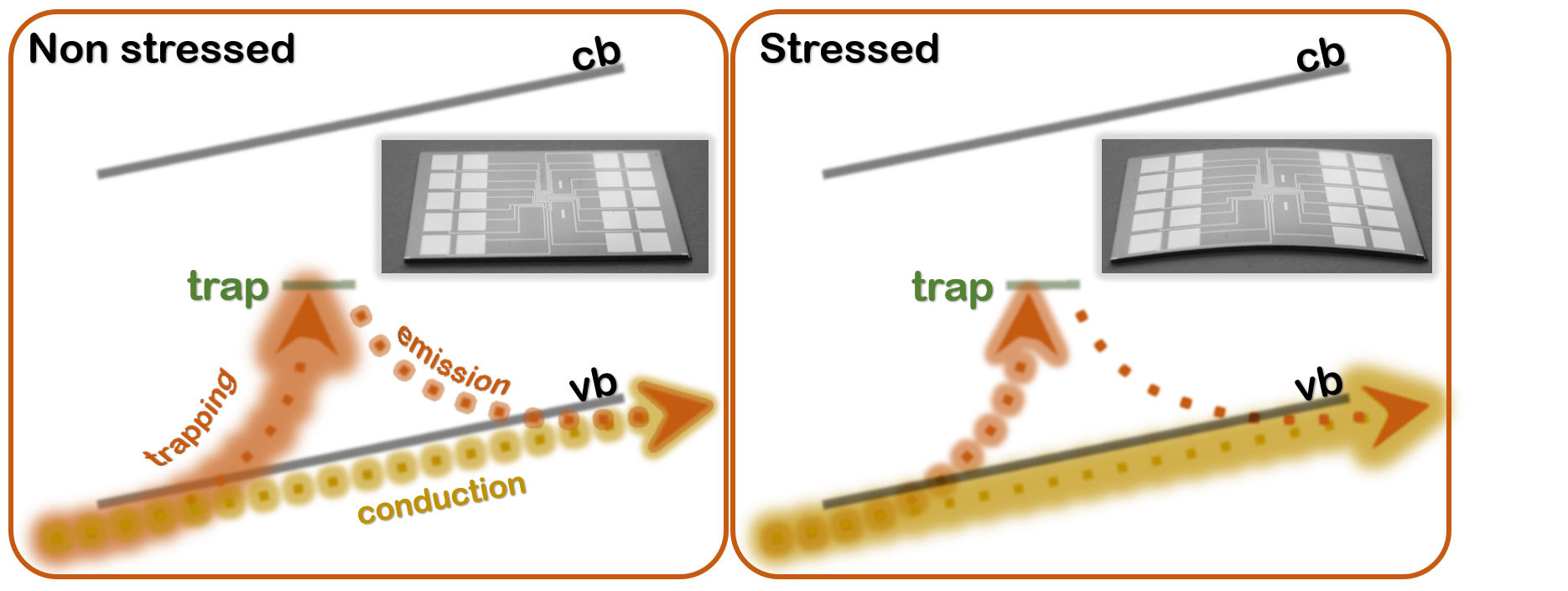
The electrical resistance of a commercial silicon wafer has been shown to exhibit giant changes when mechanically stressed. The ability to change silicon’s electrical resistance with stress, an effect known as piezo-resistance, is at the heart of strained-silicon technologies that are found in many modern, microelectronic devices. In this new work, the authors report a piezo-resistance in fully-depleted silicon-on-insulator (FD-SOI) that is more than 10 times larger than that exploited in today’s strained-silicon technologies, and they show that it is due to the electromechanical properties of crystal defects within the silicon. Importantly, the effect only appears when the resistance is measured at frequencies corresponding to the typical rates at which these crystal defects trap free electrons – those which contribute to electrical conduction – in the silicon. Under the usual DC or zero-frequency measurement conditions, the same wafer exhibits just the usual strained-silicon behaviour. As such, the result sheds new light on the debate over the piezo-resistance of silicon nanowires where are large variety of contradictory effects have been reported, and opens the way to a range of strained defect technologies such as ultra-sensitive strain sensors, fast switching diodes or electrical readout schemes for quantum technologies.