A collaboration between research groups at C2N, Synchrotron SOLEIL, LSI and PMC on the “plateau de Saclay” and of the UPMC in Paris obtained a precise determination of the electronic structure of InSe. The results were obtained combining scanning tunneling spectroscopy (STS), two-photon photoemission spectroscopy (2PPE), angle resolved photoemission spectroscopy (ARPES) and Density Functional Theory (DFT) calculations.
Physical Review Materials 3,034004 (2019)
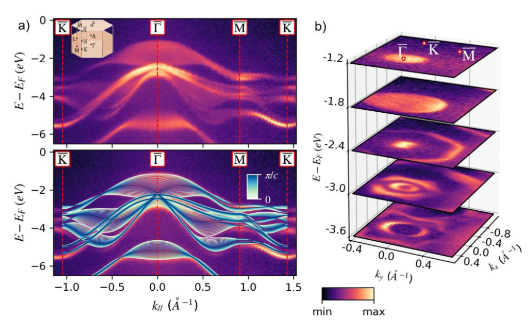
In the left part of the image we compare the high resolution map of the electronic band structure of InSe crystals collected at hν = 60 eV and T = 50 K along the 𝐾𝛤𝑀𝐾̅̅̅̅̅̅̅̅̅ direction (top) with the theoretical band structure of InSe in white-blue color scale (bottom). In the right part of the image are presented the Isoenergy contours along the 𝛤𝐾𝑀̅̅̅̅̅̅̅ plane. These findings allow a deeper understanding of the InSe electronic properties underlying the potential of III−VI semiconductors for electronic and photonic technologies.
Ref: H. Henck, D. Pierucci, J. Zribi, F. Bisti, E. Papalazarou, J. C. Girard, J. Chaste1, F. Bertran, P. Le Fevre, F. Sirotti, L. Perfetti, C. Giorgetti, A. Shukla, J. E. Rault and A. Ouerghi1 Physical Review Materials 3,034004 (2019)