Contacts: Fabian Cadiz, Fausto Sirotti
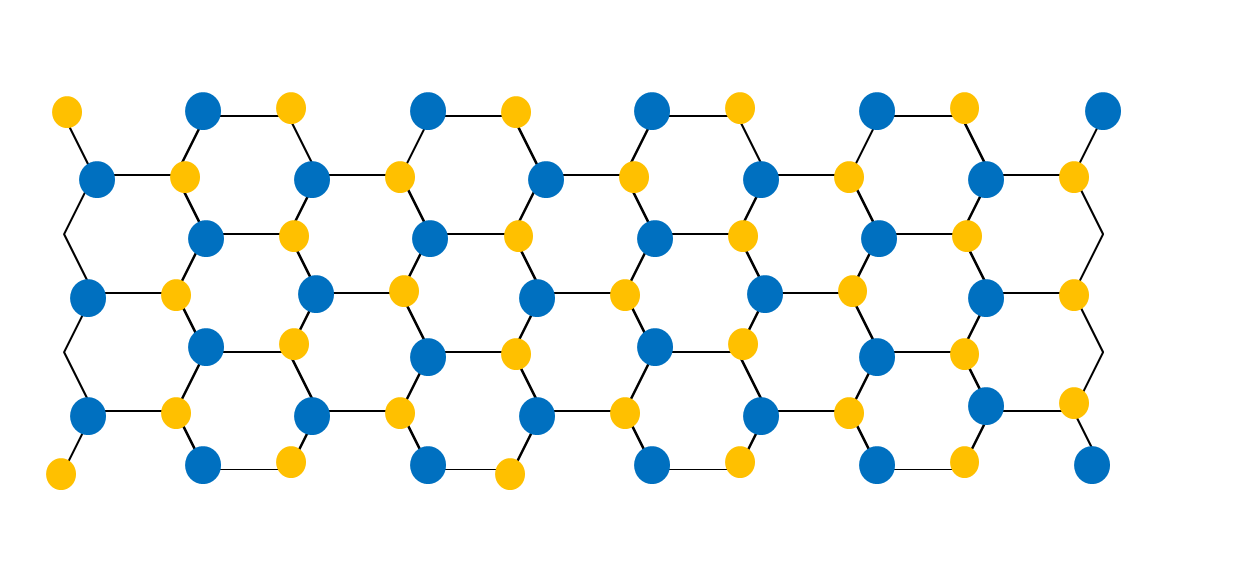
Regarding the electron spin, a remarkable property of TMDs is linked to their unique electronic band structure in the 2D limit. The interplay between broken inversion symmetry and a strong spin-orbit interaction leads to a unique spin texture of the K+ and K- valleys (the corners of the hexagonal Brillouin zone), precisely where the bandgap is located at. In a given valley and at a fixed energy, an electron can have only one possible spin state. Our research focus on the study of the optical and transport properties of spins in these atomically thin semiconductors and their heterostructures. This includes the study of spin/valley dynamics through polarized-luminescence and scanning tunneling microscopy, with an eye towards revealing original effects arising from the quantum nature of electrons at low temperatures and high densities. For more information contact Fabian Cadiz.
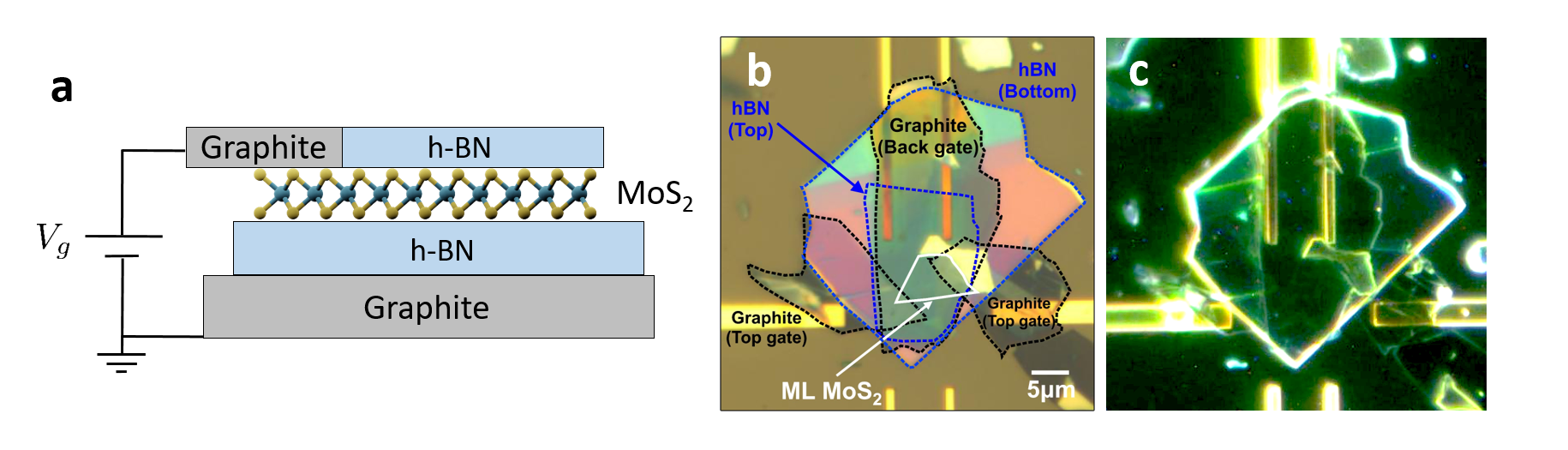
(a) Schematic side-view of an heterostructure fabricated in our lab. An MoS2 monolayer is encapsulated between two thin h-BN flakes to provide high optical quality. Thin graphite flakes were used to provide an electrical contact to the monolayer. (b) Optical microscope image of the sample under white light illumination. (c) Dark-field image of the sample, revealing clean interfaces with no visible bubbles after the formation of the heterostructure.
More information:
– Extract from Fabian Cadiz’s HDR manuscript. Download the pdf
– Article written for the journal Le Rayon of the Société Française de Physique (in French)
Current and past projects:
– ANR Project SpinCAT (2018-2023)
– ANR Project Deep2D (2022-)
– ERC Project OneSPIN (2023-)
Recent publications on 2D materials:
Imaging the effect of high photoexcited densities on valley polarization and coherence in MoS2 monolayers (2022)
F. Cadiz, S. Gerl, T. Taniguchi, K. Watanabe
npj 2d materials and applications 6, 27 (2022)
DOI: https://doi.org/10.1038/s41699-022-00303-x
Efficient valley polarization of charged excitons and resident carriers in Molybdenum disulphide monolayers by optical pumping (2022)
S. Park, S. Arscott, T. Taniguchi, K. Watanabe, F. Sirotti, F. Cadiz
Communications Physics 5, 73 (2022)
DOI: https://doi.org/10.1038/s42005-022-00850-1
Imaging Seebeck drift of excitons and trions in MoSe2 monolayers (2021)
S. Park, B. Han, C. Boule, D. Paget, A. C. H. Rowe, F. Sirotti , T. Taniguchi, K. Watanabe, C. Robert, L. Lombez, B. Urbaszek, X. Marie, F. Cadiz
2D Materials 8, 045014 (2021)
DOI: DOI: 10.1088/2053-1583/AC171F
Spin/valey pumping of resident electrons in WSe2 and WS2 monolayers (2021)
C. Robert, S. Park, F. Cadiz, L. Lombez, L. Ren, H. Tornatzky, A. Rowe, D. Paget, F. Sirotti , M. Yang, D. Van Tuan, T. Taniguchi, B. Urbaszek, K. Watanabe, T. Amand, H. Dery, X. Marie
Nature Communications 12, 5455 (2021)
DOI: DOI: 10.1038/S41467-021-25747-5
Exciton diffusion in WSe2 monolayers embedded in a van der Waals heterostructure (2018)
F. Cadiz, C. Robert, E. Courtade, M. Manca, L. Martinelli , T. Taniguchi, K. Watanabe, T. Amand, A. C. H. Rowe , D. Paget , B. Urbaszek, X. Marie
Applied Physics Letters 112, 152106 (2018)
DOI: DOI: 10.1063/1.5026478