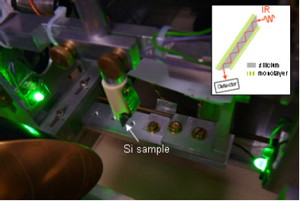
Spectroscopic characterizations : ATR- FTIR (« attenuated total reflection ») using a beveled prism of silicon to investigate surface chemistry at the solid / electrolyte interface and other environments. One specific spectrometer was built and two commercial instruments modified for in situ characterizations.
Scanning probe microscopy : In situ STM to investigate the morphology and reactivity of electrochemical interfaces. Recent developments allow fast STM imaging (a few images per second).
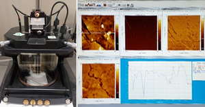
Scanning probe microscopy : AFM, mostly used ex situ to characterize surfaces in contact or non-contact mode. Conductivity and MFM are available). The electrochemical nanolithography was implemented on a modified commercial AFM.
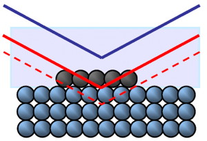
Structural characterizations : X-ray diffraction and reflectivity of thin layers using the diffractometers of the Diffrax plateforme of the Ecole Polytechnique (https://portail.polytechnique.edu/diffrax/fr). In situ characterizations are undertaken at Synchrotron radiation sources (ESRF, SOLEIL, DESY).
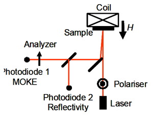
Magnetic characterizations using magneto optical Kerr effect : We perform in situ real time characterizations to determine the magnetic properties of growing ultrathin layers. We also investigate magnetoelectric coupling.
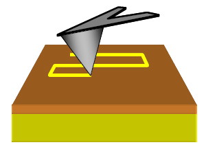
Electrochemical nanolithography : This technique allows nanostructuring in one single step and without application of a mask a metallic film by application of very short voltage pulses between a conductive AFM tip and the surface. A 4-electrode cell is used.
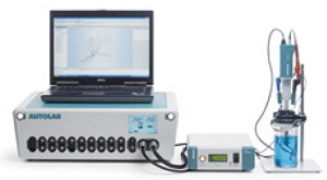
Electrochemical characterizations : voltammetry, impedance spectroscopy, RDE, QCMB.
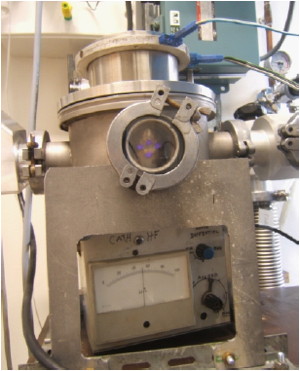
PECVD : a custom deposition chamber is designed to grow amorphous silicon and carbonated amorphous silicon layers. The power density is typically 0.1 W.cm![]() . Deposition is performed at 250°C with a pressure of 35 mTorr and a gas flow of 2L/h.
. Deposition is performed at 250°C with a pressure of 35 mTorr and a gas flow of 2L/h.
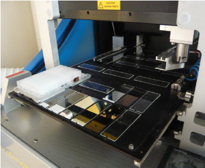
Biochips : Two spotters are available. One is spotting without contact to the surface (Arrayjet Sprint Microarrayer (V ≈ pL) ; the other is spotting with contact to the surface (BioRobotics MicroGrid II (V ≈ nL). Fluorescence is measured with a DiagArray scanner and a Hyblive imaging system (Genewave) is used to measure fluorescence in situ and in real time.