Light-emitting diodes are nowadays increasingly used, and, if widely implemented in general lighting with an energy conversion efficiency of 80%, would save 10% of the electricity consumed worldwide. However, the competing physical mechanisms involved in their operation are still hotly debated, as well as the origin of their limitations. The non radiative recombination of carriers, the large electric fields due to piezoelectric effect of these materials, and the decrease in external quantum efficiency with increasing drive current (the “efficiency droop”) all contribute to a significant reduction of the light output efficiency compared to the theoretical limits of electricity to light conversion efficiency. These complex effects are greatly modified by the intrinsic compositional inhomogeneity of the alloy material (InxGa1-xN) composing the LED active region in the form of quantum wells. This disorder at the atomic scale triggers in particular localization of the charge carriers at the nanometer scale that can significantly alter the light emitting efficiency of such structures to transform electricity into light (the quantum yield). Accounting for this phenomenon usually requires solving simultaneously in a coupled manner the Schrödinger equation describing the electronic quantum states in the disordered material, the Poisson equation describing the material internal electric fields, and the classical electron and hole transport equations in semiconductors. The simulation of one bias point in a realistic structure could easily demand several days, or even weeks of computation time.
Collaboration between two groups of the laboratory, the Electrons-Photons-Surfaces group and the Physics of Irregular Systems group, in a project involving also the National Taiwan University and the University of California at Santa Barbara, has led to the development of a fundamentally new modeling of the distribution and transport of charge carriers in disordered semiconductors, and has been applied to full LED structures. This model, intermediate between the classical “drift-diffusion” model and very advanced models directly solving the Schrödinger equation, allows one to simulate in a few minutes or hours realistic structures of several tens of microns wide, while accounting at the same time for quantum effects at the nanometer scale. It accelerates by a thousand the computational times compared to solving the standard Schrödinger equation. It provides for the first time a tool for understanding the role of nanometer disorder in these devices and paves the way to their complete design and optimization, in other words, to a real “engineering of disorder”. This work has been published in a series of 3 consecutive articles in Physical Review B in April 2017.
1 M. Filoche, M. Piccardo, Y.-R. Wu, C.-K. Li, C. Weisbuch, S. Mayboroda, “Localization landscape theory of disorder in semiconductors I : Theory and modeling”, Phys. Rev. B 95, 144204 (2017).
doi:10.1103/PhysRevB.95.144204
2 M. Piccardo, C.-K. Li, Y.-R. Wu, P. Petroff, J. S. Speck, B. Farrell, B. Yonkee, E. Young, S. Mayboroda, M. Filoche, L. Martinelli, J. Peretti, C. Weisbuch, “Urbach tails of disordered InxGa1-xN quantum well layers : Experiments and theory”, Phys. Rev. B, 95, 144205 (2017). doi:10.1103/PhysRevB.95.144205
3 C.-K. Li, M. Piccardo, L.-S. Lu, S. Mayboroda, L. Martinelli, J. S. Speck, C. Weisbuch, M. Filoche, Y.-R. Wu, “Localization landscape theory of disorder in semiconductors III : Application to carrier transport and recombination in light emitting diodes”, Phys. Rev. B, 95, 144206 (2017).
doi:10.1103/PhysRevB.95.144206

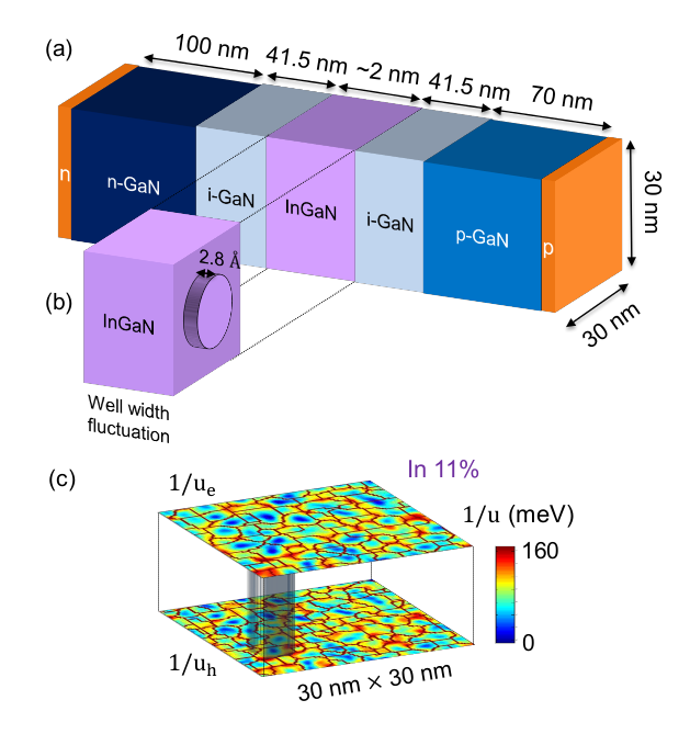
Top : Structure and composition of a quantum well structure studied using the new developed model.
Bottom : the localization landscape theory provides two maps of the localization regions of electrons and holes, allowing assessing their overlaps and from there to compute accurately the radiative and non radiative recombination rates.


